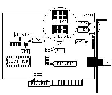
COMPEX, INC.
ANET-1, ANET-12
|
NIC Type |
ARCnet |
|
Transfer Rate |
2.5Mbps |
|
Data Bus |
8-bit ISA |
|
Topology |
Star (ANET-1) Linear Bus (ANET-12) |
|
Wiring Type |
RG-62A/U 93ohm coaxial |
|
Boot ROM |
Available |

|
NODE ADDRESS |
||||||||
|
Node |
SW1/1 |
SW1/2 |
SW1/3 |
SW1/4 |
SW1/5 |
SW1/6 |
SW1/7 |
SW1/8 |
|
0 |
- |
- |
- |
- |
- |
- |
- |
- |
|
1 |
Off |
On |
On |
On |
On |
On |
On |
On |
|
2 |
On |
Off |
On |
On |
On |
On |
On |
On |
|
3 |
Off |
Off |
On |
On |
On |
On |
On |
On |
|
4 |
On |
On |
Off |
On |
On |
On |
On |
On |
|
251 |
Off |
Off |
On |
Off |
Off |
Off |
Off |
Off |
|
252 |
On |
On |
Off |
Off |
Off |
Off |
Off |
Off |
|
253 |
Off |
On |
Off |
Off |
Off |
Off |
Off |
Off |
|
254 |
On |
Off |
Off |
Off |
Off |
Off |
Off |
Off |
|
255 |
Off |
Off |
Off |
Off |
Off |
Off |
Off |
Off |
|
Note:Node address 0 is used for messaging between nodes and must not be used. A total of 255 node address settings are available. The switches are a binary representation of the decimal node addresses. Switch 1 is the Least Significant Bit and switch 8 is the Most Significant Bit. The switches have the following decimal values: switch 1=1, 2=2, 3=4, 4=8, 5=16, 6=32, 7=64, 8=128. Turn off the switches and add the values of the off switches to obtain the correct node address. (On=0, Off=1) |
||||||||
|
RESPONSE AND RECONFIGURATION TIMEOUTS |
|||||
|
Response Time |
Idle Time |
Reconfiguration Time |
JP1 |
JP2 |
|
|
» |
74.7µs |
86µs |
840ms |
Open |
Open |
|
|
283.4µs |
316µs |
1680ms |
Open |
Closed |
|
|
561.8µs |
624µs |
1680ms |
Closed |
Open |
|
|
1118.6µs |
1237µs |
1680ms |
Closed |
Closed |
|
Note:All NICs on the network segment must have this option set the same. |
|||||
|
MODE SELECTION |
||
|
Mode |
JP3 |
|
|
» |
Normal |
As shown in diagram on previous page |
|
|
Special |
As shown on diagram on previous page |
Note:In normal mode, any 32KB memory segment in the system may be selected. For an AT, however, with memory, display cards, and a hard drive controller, only 16KB of free memory space is available between CC000h and CFFFFh. In Special Mode the memory space occupied by the adapter is reduced by half to 16KB and the memory address is automatically set to CC000h. This overrides the base memory setting on JP15 and JP16. |
||
|
I/O BASE ADDRESS |
|||||||
|
Address |
JP9 |
JP8 |
JP7 |
JP6 |
JP5 |
JP4 |
|
|
|
260h |
Open |
Closed |
Closed |
Open |
Open |
Closed |
|
|
280h |
Open |
Closed |
Open |
Closed |
Closed |
Closed |
|
» |
2E0h |
Open |
Closed |
Open |
Open |
Open |
Closed |
|
|
2F0h |
Open |
Closed |
Open |
Open |
Open |
Open |
|
|
300h |
Open |
Open |
Closed |
Closed |
Closed |
Closed |
|
|
360h |
Open |
Open |
Closed |
Open |
Open |
Closed |
|
Note:Jumpers count from right to left in the diagram. |
|||||||
|
INTERRUPT REQUEST |
||||||
|
IRQ |
JP10 |
JP11 |
JP12 |
JP13 |
JP14 |
|
|
» |
2/9 |
Closed |
Open |
Open |
Open |
Open |
|
|
3 |
Open |
Closed |
Open |
Open |
Open |
|
|
4 |
Open |
Open |
Closed |
Open |
Open |
|
|
5 |
Open |
Open |
Open |
Closed |
Open |
|
|
7 |
Open |
Open |
Open |
Open |
Closed |
|
BOOT ROM ADDRESS |
||||||
|
Address |
JP15 |
JP16 |
JP17 |
JP18 |
JP19 |
|
|
|
C0000h |
Closed |
Closed |
Closed |
Open |
Open |
|
|
C8000h |
Open |
Closed |
Closed |
Open |
Open |
|
|
CC000h |
Open |
Open |
Closed |
Open |
Open |
|
» |
D0000h |
Closed |
Open |
Closed |
Open |
Open |
|
Note:Jumpers count from the bottom up in the diagram. |
||||||
|
DIAGNOSTIC LED(S) |
|||
|
LED |
Color |
Status |
Condition |
|
LED1 |
Red |
On |
Data is being transmitted |
|
LED1 |
Red |
Off |
Data is not being transmitted |
|
LED2 |
Green |
On |
Data is being received |
|
LED2 |
Green |
Off |
Data is not being received |