TEKNOR INDUSTRIAL COMPUTERS, INC.
TEK933
|
Device Type |
Mainboard |
|
Processor |
Pentium |
|
Processor Speed |
75/90/100/120/133/150/166/200MHz |
|
Chip Set |
Intel |
|
Video Chip Set |
Unidentified |
|
Maximum Onboard Memory |
256MB (EDO supported) |
|
Maximum Video Memory |
2MB |
|
Cache |
256KB |
|
BIOS |
AMI |
|
Dimensions |
339mm x 122mm |
|
I/O Options |
Ethernet 10Base2 connector, Ethernet 10BaseT connector, floppy drive interface, IDE interfaces (2), SCSI interface, parallel port, PS/2 mouse port, serial ports (2), flat panel connector |
|
NPU Options |
None |

|
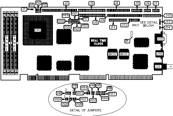
CONNECTIONS | |||
|
Purpose |
Location |
Purpose |
Location |
|
External battery |
B1 |
Flat panel connector |
J9 |
|
Chassis fan power |
J1 |
Parallel port |
J10 |
|
SCSI interface |
J2 |
VGA feature connector |
J11 |
|
IDE interface 1 |
J3 |
Analog encoder connector |
J12 |
|
Floppy drive interface |
J4 |
PS/2 mouse port |
J13 |
|
Multi function connector |
J5 |
VGA port |
J15 |
|
Serial port 1 |
J6 |
Ethernet 10Base2 connector |
J16 |
|
Serial port 2 |
J7 |
Ethernet 10BaseT connector |
J23 |
|
IDE interface 2 |
J8 | ||
|
USER CONFIGURABLE SETTINGS | |||
|
Function |
Label |
Position | |
|
BIOS boot select normal |
J14 |
Open | |
|
BIOS boot select recovery mode |
J14 |
Closed | |
|
» |
Factory configured - do not alter |
W8/pins 1 & 2 |
Open |
|
» |
Standard mode enabled |
W8/pins 3 & 4 |
Open |
|
VT100 mode enabled |
W8/pins 3 & 4 |
Closed | |
|
» |
Teknor extension disabled |
W8/pins 5 & 6 |
Closed |
|
Teknor extension enabled |
W8/pins 5 & 6 |
Open | |
|
» |
On board video enabled |
W8/pins 7 & 8 |
Open |
|
On board video disabled |
W8/pins 7 & 8 |
Closed | |
|
» |
Non maskable interrupt on power fail output disabled |
W13 |
Open |
|
Non maskable interrupt on power fail output enabled |
W13 |
Closed | |
|
» |
Panel shift clock normal |
W22 |
Pins 1 & 2 closed |
|
Panel shift clock inverse |
W22 |
Pins 2 & 3 closed | |
|
» |
Watchdog timer enabled |
W26 |
Closed |
|
Watchdog timer disabled |
W26 |
Open | |
|
» |
Internal battery disabled |
W27 |
Open |
|
Internal battery enabled |
W27 |
Closed | |
|
SIMM CONFIGURATION | ||
|
Size |
Bank 0 |
Bank 1 |
|
2MB |
(2) 256K x 36 |
None |
|
4MB |
(2) 512K x 36 |
None |
|
4MB |
(2) 256K x 36 |
(2) 256K x 36 |
|
6MB |
(2) 512K x 36 |
(2) 256K x 36 |
|
8MB |
(2) 1M x 36 |
None |
|
SIMM CONFIGURATION (CON’T) | ||
|
Size |
Bank 0 |
Bank 1 |
|
8MB |
(2) 512K x 36 |
(2) 512K x 36 |
|
10MB |
(2) 1M x 36 |
(2) 256K x 36 |
|
12MB |
(2) 512K x 36 |
(2) 1M x 36 |
|
16MB |
(2) 2M x 36 |
None |
|
16MB |
(2) 1M x 36 |
(2) 1M x 36 |
|
18MB |
(2) 2M x 36 |
(2) 256K x 36 |
|
20MB |
(2) 512K x 36 |
(2) 2M x 36 |
|
24MB |
(2) 2M x 36 |
(2) 1M x 36 |
|
32MB |
(2) 4M x 36 |
None |
|
32MB |
(2) 2M x 36 |
(2) 2M x 36 |
|
34MB |
(2) 4M x 36 |
(2) 256K x 36 |
|
36MB |
(2) 512K x 36 |
(2) 4M x 36 |
|
40MB |
(2) 4M x 36 |
(2) 1M x 36 |
|
48MB |
(2) 2M x 36 |
(2) 4M x 36 |
|
64MB |
(2) 8M x 36 |
None |
|
64MB |
(2) 4M x 36 |
(2) 4M x 36 |
|
66MB |
(2) 8M x 36 |
(2) 256K x 36 |
|
68MB |
(2) 512K x 36 |
(2) 8M x 36 |
|
72MB |
(2) 8M x 36 |
(2) 1M x 36 |
|
80MB |
(2) 2M x 36 |
(2) 8M x 36 |
|
96MB |
(2) 8M x 36 |
(2) 4M x 36 |
|
128MB |
(2) 8M x 36 |
(2) 8M x 36 |
|
128MB |
(2) 16M x 36 |
None |
|
130MB |
(2) 16M x 36 |
(2) 256K x 36 |
|
132MB |
(2) 16M x 36 |
(2) 512K x 36 |
|
136MB |
(2) 16M x 36 |
(2) 1M x 36 |
|
144MB |
(2) 16M x 36 |
(2) 2M x 36 |
|
160MB |
(2) 16M x 36 |
(2) 4M x 36 |
|
192MB |
(2) 16M x 36 |
(2) 8M x 36 |
|
256MB |
(2) 16M x 36 |
(2) 16M x 36 |
|
Note: Board accepts EDO memory. | ||
|
CACHE CONFIGURATION | ||
|
Size |
Bank 0 |
Bank 1 |
|
256KB |
(4) 32K x 8 |
(4) 32K x 8 |
|
1MB |
(4) 128K x 8 |
(4) 128K x 8 |
|
Note: The cache is located on the underside of the card. | ||
|
CACHE TYPE CONFIGURATION | ||
|
Type |
W1 | |
| » |
Write back |
Pins 1 & 2 closed |
|
Write through |
Pins 2 & 3 closed | |
|
VIDEO MEMORY CONFIGURATION |
|
Note: Board accepts 1MB/2MB of video memory. The location and chip types are unidentified. |
|
CPU SPEED SELECTION | |||||||
|
CPU speed |
Clock speed |
Multiplier |
W2 |
W3 |
W19 |
W20 |
W21 |
|
75MHz |
50MHz |
1.5x |
1 & 2 |
1 & 2 |
2 & 3 |
1 & 2 |
2 & 3 |
|
90MHz |
60MHz |
1.5x |
1 & 2 |
1 & 2 |
1 & 2 |
1 & 2 |
1 & 2 |
|
100MHz |
66MHz |
1.5x |
1 & 2 |
1 & 2 |
1 & 2 |
2 & 3 |
2 & 3 |
|
120MHz |
60MHz |
2x |
1 & 2 |
2 & 3 |
1 & 2 |
1 & 2 |
1 & 2 |
|
133MHz |
66MHz |
2x |
1 & 2 |
2 & 3 |
1 & 2 |
2 & 3 |
2 & 3 |
|
150MHz |
60MHz |
2.5x |
2 & 3 |
2 & 3 |
1 & 2 |
1 & 2 |
1 & 2 |
|
166MHz |
66MHz |
2.5x |
2 & 3 |
2 & 3 |
1 & 2 |
2 & 3 |
2 & 3 |
|
Note: Pins designated should be in the closed position. | |||||||
|
SERIAL PORT 2 LOOPBACK SELECTION | |||
|
Setting |
W4 |
W15 | |
| » |
Normal |
Open |
Open |
|
Loopback |
Closed |
Closed | |
|
SERIAL PORT 2 SELECTION | ||||||
|
Setting |
W5 |
W6 |
W14 |
W16 |
W17 | |
| » |
RS-232 |
1 & 2 |
1 & 2 |
Open |
1 & 2 |
1 & 2 |
|
RS-485/422 |
2 & 3 |
2 & 3 |
Closed |
2 & 3 |
2 & 3 | |
|
Note: Pins designated should be in the closed position. | ||||||
|
FLOPPY DRIVE EDOUT SELECTION | ||
|
Setting |
W24 | |
| » |
Left to software |
Open |
|
Ground to pin 17 on J4 |
Pins 2 & 4 closed | |
|
Ground to pin 29 on J4 |
Pins 3 & 4 closed | |
|
EDOUT to pin 29 on J4 |
Pins 1 & 3 closed | |
|
EDOUT to pin 17 on J4 |
Pins 1 & 2 closed | |
|
FLOPPY DRIVE HDOUT SELECTION | ||
|
Setting |
W25 | |
| » |
Left to software |
Open |
|
Ground to pin 27 on J4 |
Pins 2 & 4 closed | |
|
Ground to pin 33 on J4 |
Pins 3 & 4 closed | |
|
HDOUT to pin 33 on J4 |
Pins 1 & 3 closed | |
|
HDOUT to pin 27 on J4 |
Pins 1 & 2 closed | |
|
BASE I/O SELECTION | ||
|
Address |
W9 | |
| » |
190H |
Pins 1 & 2, 3 & 4 closed |
|
290H |
Pins 1 & 2 closed | |
|
390H |
Pins 3 & 4 closed | |
|
390H |
Open | |
|
SCSI TERMINATION SELECTION | ||
|
Setting |
W18 | |
| » |
Controlled by hardware |
Pins 2 & 3 closed |
|
Controlled by software |
Pins 1 & 2 closed | |
|
Disabled by hardware |
Open | |
|
FEATURE/VIDEO STANDBY SELECTION | |||
|
Setting |
W7 |
W23 | |
| » |
Feature connector disabled/video standby enabled |
Closed |
Open |
|
Feature connector enabled/video standby disabled |
Open |
Closed | |