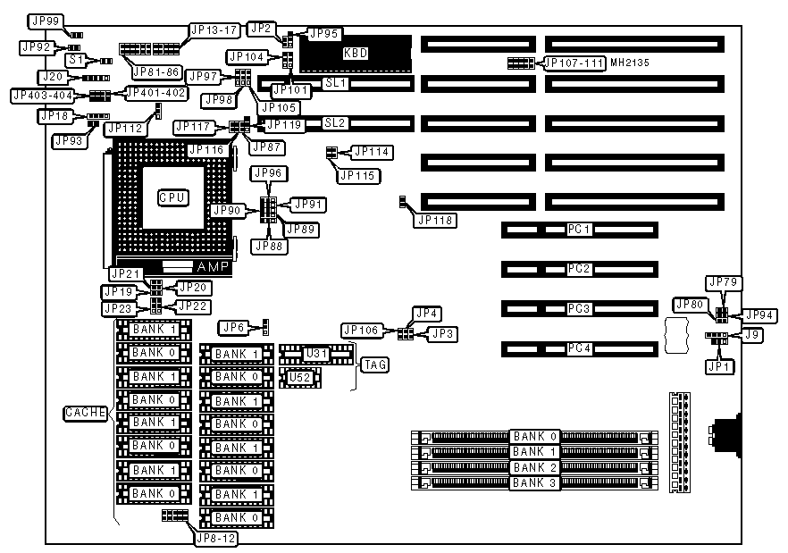
SUPER MICRO
P54VL-PCI
|
Processor |
Pentium |
|
Processor Speed |
90/100MHz |
|
Chip Set |
OPTI |
|
Max. Onboard DRAM |
128MB |
|
Cache |
128/256/512KB |
|
BIOS |
AMI |
|
Dimensions |
330mm x 218mm |
|
I/O Options |
32-bit PCI bus slots (4), 32-bit VESA local bus slots (2), green PC connector |
|
NPU Options |
None |

|
CONNECTIONS | |||
|
Purpose |
Location |
Purpose |
Location |
|
External battery |
J9 |
Green PC connector (power supply) |
JP94 |
|
Power LED & keylock |
J20 |
Turbo LED |
JP99 |
|
Speaker |
JP18 |
32-bit PCI bus slots |
PC1 - PC4 |
|
Green PC connector (peripheral) |
JP79 |
Reset switch |
S1 |
|
Green PC connector (peripheral) |
JP80 |
32-bit VESA local bus slots |
SL1 & SL2 |
|
Turbo switch |
JP92 | ||
|
USER CONFIGURABLE SETTINGS | |||
|
Function |
Jumper |
Position | |
|
» |
CMOS memory normal operation |
JP1 |
pins 2 & 3 closed |
|
CMOS memory clear |
JP1 |
pins 1 & 2 closed | |
|
» |
Factory configured - do not alter |
JP2 |
Open |
|
» |
Factory configured - do not alter |
JP3 |
Open |
|
» |
Factory configured - do not alter |
JP4 |
Closed |
|
» |
Factory configured - do not alter |
JP8 |
Open |
|
» |
Factory configured - do not alter |
JP9 |
Closed |
|
» |
Factory configured - do not alter |
JP10 |
Closed |
|
» |
Factory configured - do not alter |
JP11 |
Open |
|
» |
Factory configured - do not alter |
JP12 |
Open |
|
» |
Factory configured - do not alter |
JP13 |
Open |
|
» |
Factory configured - do not alter |
JP14 |
Open |
|
» |
Factory configured - do not alter |
JP15 |
Closed |
|
» |
Factory configured - do not alter |
JP16 |
Closed |
|
» |
Factory configured - do not alter |
JP17 |
Closed |
|
» |
Factory configured - do not alter |
JP77 |
Open |
|
» |
Factory configured - do not alter |
JP81 |
Open |
|
» |
Factory configured - do not alter |
JP82 |
Closed |
|
» |
Factory configured - do not alter |
JP83 |
Closed |
|
» |
Factory configured - do not alter |
JP84 |
Open |
|
» |
Factory configured - do not alter |
JP85 |
Closed |
|
» |
Factory configured - do not alter |
JP86 |
Open |
|
» |
Factory configured - do not alter |
JP87 |
Open |
|
» |
Factory configured - do not alter |
JP88 |
pins 2 & 3 closed |
|
» |
Factory configured - do not alter |
JP89 |
pins 1 & 2 closed |
|
» |
Factory configured - do not alter |
JP90 |
pins 1 & 2 closed |
|
» |
Factory configured - do not alter |
JP91 |
pins 1 & 2 closed |
|
» |
Factory configured - do not alter |
JP93 |
Open |
|
» |
Factory configured - do not alter |
JP95 |
pins 2 & 3 closed |
|
» |
Factory configured - do not alter |
JP96 |
pins 1 & 2 closed |
|
» |
Factory configured - do not alter |
JP97 |
pins 1 & 2 closed |
|
» |
Factory configured - do not alter |
JP98 |
pins 1 & 2 closed |
|
» |
Factory configured - do not alter |
JP101 |
pins 1 & 2 closed |
|
» |
Factory configured - do not alter |
JP104 |
pins 1 & 2 closed |
|
» |
Factory configured - do not alter |
JP105 |
pins 1 & 2 closed |
|
» |
Factory configured - do not alter |
JP106 |
Open |
|
» |
Factory configured - do not alter |
JP114 |
Open |
|
» |
Factory configured - do not alter |
JP115 |
Open |
|
» |
Factory configured - do not alter |
JP116 |
Open |
|
» |
Factory configured - do not alter |
JP117 |
Open |
|
» |
Factory configured - do not alter |
JP118 |
Open |
|
» |
Factory configured - do not alter |
JP119 |
pins 2 & 3 closed |
|
» |
Factory configured - do not alter |
JP401 |
Closed |
|
USER CONFIGURABLE SETTINGS (CON’T) | |||
|
Function |
Jumper |
Position | |
|
» |
Factory configured - do not alter |
JP402 |
Open |
|
» |
Factory configured - do not alter |
JP403 |
Open |
|
» |
Factory configured - do not alter |
JP404 |
Open |
|
Note: The location of JP77 is unidentified. | |||
|
DRAM CONFIGURATION | ||||
|
Size |
Bank 0 |
Bank 1 |
Bank 2 |
Bank 3 |
|
2MB |
(1) 256K x 36 |
(1) 256K x 36 |
NONE |
NONE |
|
4MB |
(1) 512K x 36 |
(1) 512K x 36 |
NONE |
NONE |
|
4MB |
(1) 256K x 36 |
(1) 256K x 36 |
(1) 256K x 36 |
(1) 256K x 36 |
|
6MB |
(1) 256K x 36 |
(1) 256K x 36 |
(1) 512K x 36 |
(1) 512K x 36 |
|
8MB |
(1) 1M x 36 |
(1) 1M x 36 |
NONE |
NONE |
|
8MB |
(1) 512K x 36 |
(1) 512K x 36 |
(1) 512K x 36 |
(1) 512K x 36 |
|
10MB |
(1) 256K x 36 |
(1) 256K x 36 |
(1) 1M x 36 |
(1) 1M x 36 |
|
12MB |
(1) 512K x 36 |
(1) 512K x 36 |
(1) 1M x 36 |
(1) 1M x 36 |
|
16MB |
(1) 2M x 36 |
(1) 2M x 36 |
NONE |
NONE |
|
16MB |
(1) 1M x 36 |
(1) 1M x 36 |
(1) 1M x 36 |
(1) 1M x 36 |
|
18MB |
(1) 256K x 36 |
(1) 256K x 36 |
(1) 2M x 36 |
(1) 2M x 36 |
|
20MB |
(1) 512K x 36 |
(1) 512K x 36 |
(1) 2M x 36 |
(1) 2M x 36 |
|
24MB |
(1) 1M x 36 |
(1) 1M x 36 |
(1) 2M x 36 |
(1) 2M x 36 |
|
32MB |
(1) 4M x 36 |
(1) 4M x 36 |
NONE |
NONE |
|
32MB |
(1) 2M x 36 |
(1) 2M x 36 |
(1) 2M x 36 |
(1) 2M x 36 |
|
34MB |
(1) 256K x 36 |
(1) 256K x 36 |
(1) 4M x 36 |
(1) 4M x 36 |
|
36MB |
(1) 512K x 36 |
(1) 512K x 36 |
(1) 4M x 36 |
(1) 4M x 36 |
|
40MB |
(1) 1M x 36 |
(1) 1M x 36 |
(1) 4M x 36 |
(1) 4M x 36 |
|
48MB |
(1) 2M x 36 |
(1) 2M x 36 |
(1) 4M x 36 |
(1) 4M x 36 |
|
64MB |
(1) 4M x 36 |
(1) 4M x 36 |
(1) 4M x 36 |
(1) 4M x 36 |
|
64MB |
(1) 8M x 36 |
(1) 8M x 36 |
NONE |
NONE |
|
66MB |
(1) 256K x 36 |
(1) 256K x 36 |
(1) 8M x 36 |
(1) 8M x 36 |
|
68MB |
(1) 512K x 36 |
(1) 512K x 36 |
(1) 8M x 36 |
(1) 8M x 36 |
|
72MB |
(1) 1M x 36 |
(1) 1M x 36 |
(1) 8M x 36 |
(1) 8M x 36 |
|
80MB |
(1) 2M x 36 |
(1) 2M x 36 |
(1) 8M x 36 |
(1) 8M x 36 |
|
96MB |
(1) 4M x 36 |
(1) 4M x 36 |
(1) 8M x 36 |
(1) 8M x 36 |
|
128MB |
(1) 8M x 36 |
(1) 8M x 36 |
(1) 8M x 36 |
(1) 8M x 36 |
|
CACHE CONFIGURATION | ||||
|
Size |
Bank 0 |
Bank 1 |
TAG (U31) |
Dirty bit (U52) |
|
128KB |
(8) 8K x 8 |
(8) 8K x 8 |
(1) 32K x 8 |
(1) 16K x 1 |
|
256KB |
(8) 32K x 8 |
NONE |
(1) 32K x 8 |
(1) 16K x 1 |
|
512KB |
(8) 32K x 8 |
(8) 32K x 8 |
(1) 32K x 8 |
(1) 16K x 1 |
|
CACHE JUMPER CONFIGURATION | ||||||
|
Size |
JP6 |
JP19 |
JP20 |
JP21 |
JP22 |
JP23 |
|
128KB |
2 & 3 |
Closed |
Open |
Open |
2 & 3 |
2 & 3 |
|
256KB |
1 & 2 |
Closed |
Closed |
Open |
1 & 2 |
1 & 2 |
|
512KB |
2 & 3 |
Closed |
Closed |
Closed |
2 & 3 |
2 & 3 |
|
Note: Pins designated should be in the closed position. | ||||||
|
CPU SPEED CONFIGURATION | |
|
Speed |
JP112 |
|
90MHz |
pins 1 & 2 closed |
|
100MHz |
pins 2 & 3 closed |
|
INTERRUPT CONFIGURATION | |||
|
IRQ |
JP107 |
JP108 |
JP109 |
|
IRQ3 |
Closed |
Open |
Open |
|
IRQ4 |
Open |
Closed |
Open |
|
IRQ9 |
Open |
Open |
Closed |
|
Note: Only one jumper at a time can be closed in jumper block JP107-111. | |||
|
VIDEO CARD CONFIGURATION | ||
|
Video card |
JP110 |
JP111 |
|
ISA |
Closed |
Open |
|
Local bus |
Open |
Closed |
|
Note: Only one jumper at a time can be closed in jumper block JP107-111. | ||