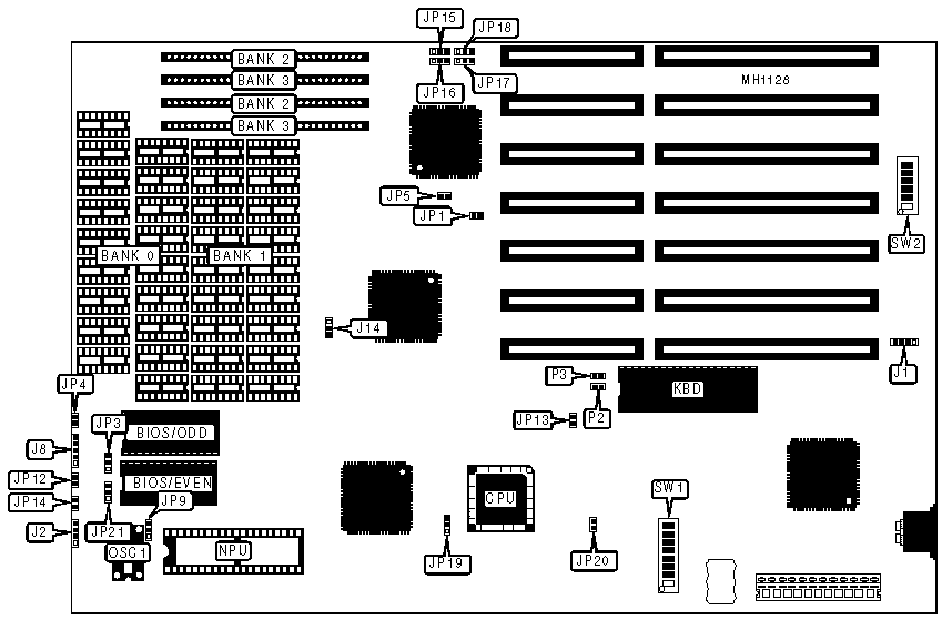
SINGA
286G
|
Processor |
80286 |
|
Processor Speed |
12MHz |
|
Chip Set |
GC |
|
Max. Onboard DRAM |
8MB |
|
Cache |
None |
|
BIOS |
Quadtel |
|
Dimensions |
330mm x 218mm |
|
I/O Options |
None |
|
NPU Options |
80287 |

|
CONNECTIONS | |||
|
Purpose |
Location |
Purpose |
Location |
|
External battery |
J1 |
Reset switch |
JP4 |
|
Speaker |
J2 |
Turbo LED |
JP12 |
|
Power LED & keylock |
J8 |
Turbo switch |
JP14 |
|
USER CONFIGURABLE SETTINGS | |||
|
Function |
Jumper/Switch |
Position | |
| » |
Factory configured - do not alter |
JP1 |
N/A |
| » |
I/O wait state select one |
JP5 |
Open |
|
I/O wait states select zero |
JP5 |
Closed | |
| » |
NPU clock select synchronous with CPU |
JP9 |
pins 1 & 2 closed |
|
NPU clock select synchronous with OSC1 |
JP9 |
pins 2 & 3 closed | |
| » |
Monitor type select color |
JP13 |
Closed |
|
Monitor type select monochrome |
JP13 |
Open | |
| » |
Parity check enabled |
JP19 |
pins 1 & 2 closed |
|
Parity check disabled |
JP19 |
pins 2 & 3 closed | |
| » |
Communications port select COM1/COM2 |
JP20 |
Closed |
|
Communications port select COM3/COM4 |
JP20 |
Open | |
| » |
Enable IRQ5 for parallel port |
SW1/1 |
On |
|
Enable IRQ7 for parallel port |
SW1/2 |
On | |
| » |
Enable IRQ3 for serial port 2 |
SW1/3 |
On |
| » |
Enable IRQ4 for serial port 1 |
SW1/4 |
On |
| » |
Port select LPT1 |
SW1/5 |
On |
|
Port select LPT2 |
SW1/5 |
Off | |
| » |
Printer port 1 enabled |
SW1/6 |
On |
|
Printer port 1 disabled |
SW1/6 |
Off | |
| » |
Serial port S1 enabled |
SW1/7 |
On |
|
Serial port S1 disabled |
SW1/7 |
Off | |
| » |
Serial port S2 enabled |
SW1/8 |
On |
|
Serial port S2 disabled |
SW1/8 |
Off | |
| » |
Factory configured - do not alter |
SW2/1 |
N/A |
| » |
Memory between 640 and 1024KB available |
SW2/2 |
On |
|
Memory between 640 and 1024KB not available |
SW2/2 |
Off | |
| » |
SIMM type at Bank 0select 256K x 9 |
SW2/3 |
On |
|
SIMM type at Bank 0select 1M x 9 |
SW2/3 |
Off | |
| » |
I/O speed select slow |
SW2/6 |
On |
|
I/O speed select fast |
SW2/6 |
Off | |
|
Note:The location of I/O ports is unidentified. | |||
|
DRAM CONFIGURATION | ||||
|
Size |
Bank 0 |
Bank 1 |
Bank 2 |
Bank 3 |
|
512KB |
(18) 41256 |
NONE |
NONE |
NONE |
|
512KB |
NONE |
NONE |
(2) 256K x 9 |
NONE |
|
1MB |
(18) 41256 |
(18) 41256 |
NONE |
NONE |
|
1MB |
NONE |
NONE |
(2) 256K x 9 |
(2) 256K x 9 |
|
1.5MB |
(18) 41256 |
(18) 41256 |
(2) 256K x 9 |
NONE |
|
1.5MB |
(18) 41256 |
NONE |
(2) 256K x 9 |
(2) 256K x 9 |
|
2MB |
(18) 411000 |
NONE |
NONE |
NONE |
|
2MB |
NONE |
NONE |
(2) 1M x 9 |
NONE |
|
3MB |
(18) 411000 |
NONE |
(2) 256K x 9 |
(2) 256K x 9 |
|
4MB |
(18) 411000 |
(18) 411000 |
(2) 1M x 9 |
NONE |
|
4MB |
NONE |
NONE |
(2) 1M x 9 |
(2) 1M x 9 |
|
5MB |
(18) 411000 |
(18) 411000 |
(2) 256K x 9 |
(2) 256K x 9 |
|
5MB |
(18) 41256 |
(18) 41256 |
(2) 1M x 9 |
(2) 1M x 9 |
|
6MB |
(18) 411000 |
(18) 411000 |
(2) 1M x 9 |
NONE |
|
8MB |
(18) 411000 |
(18) 411000 |
(2) 1M x 9 |
(2) 1M x 9 |
|
DRAM CONFIGURATION | ||||
|
Size |
JP15 |
JP16 |
JP17 |
JP18 |
|
512KB |
pins 1 & 2 closed |
pins 2 & 3 closed |
pins 1 & 2 closed |
pins 2 & 3 closed |
|
512KB |
pins 2 & 3 closed |
pins 1 & 2 closed |
pins 2 & 3 closed |
pins 1 & 2 closed |
|
1MB |
pins 1 & 2 closed |
pins 2 & 3 closed |
pins 1 & 2 closed |
pins 2 & 3 closed |
|
1MB |
pins 2 & 3 closed |
pins 1 & 2 closed |
pins 2 & 3 closed |
pins 1 & 2 closed |
|
1.5MB |
pins 1 & 2 closed |
pins 2 & 3 closed |
pins 1 & 2 closed |
pins 2 & 3 closed |
|
1.5MB |
pins 2 & 3 closed |
pins 1 & 2 closed |
pins 2 & 3 closed |
pins 1 & 2 closed |
|
2MB |
pins 1 & 2 closed |
pins 2 & 3 closed |
pins 1 & 2 closed |
pins 2 & 3 closed |
|
2MB |
pins 2 & 3 closed |
pins 1 & 2 closed |
pins 2 & 3 closed |
pins 1 & 2 closed |
|
3MB |
pins 2 & 3 closed |
pins 1 & 2 closed |
pins 2 & 3 closed |
pins 1 & 2 closed |
|
4MB |
pins 1 & 2 closed |
pins 2 & 3 closed |
pins 1 & 2 closed |
pins 2 & 3 closed |
|
4MB |
pins 2 & 3 closed |
pins 1 & 2 closed |
pins 2 & 3 closed |
pins 1 & 2 closed |
|
5MB |
pins 1 & 2 closed |
pins 2 & 3 closed |
pins 1 & 2 closed |
pins 2 & 3 closed |
|
5MB |
pins 1 & 2 closed |
pins 2 & 3 closed |
pins 1 & 2 closed |
pins 2 & 3 closed |
|
6MB |
pins 1 & 2 closed |
pins 2 & 3 closed |
pins 1 & 2 closed |
pins 2 & 3 closed |
|
8MB |
pins 1 & 2 closed |
pins 2 & 3 closed |
pins 1 & 2 closed |
pins 2 & 3 closed |
|
BIOS CONFIGURATION | ||
|
Size |
JP3 |
JP21 |
|
27128 |
pins 1 & 2 closed |
pins 1 & 2 closed |
|
27256 |
pins 2 & 3 closed |
pins 2 & 3 closed |
|
27512 |
pins 2 & 3 closed |
pins 2 & 3 closed |