HAUPPAUGE COMPUTER WORKS, INC.
MODEL 486M VBB MODULAR
|
Processor |
80486DX/80486DX2 (located on an external CPU card) |
|
Processor Speed |
33/50/66(internal)MHz |
|
Chip Set |
C & T |
|
Max. Onboard DRAM |
64MB |
|
Cache |
64/128/256/1024KB (located on an external CPU card) |
|
BIOS |
MR |
|
Dimensions |
330mm x 218mm |
|
I/O Options |
32-bit external CPU cards (2), floppy drive interface, IDE interface, parallel port, serial ports (2) |
|
NPU Options |
None |

|
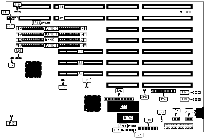
CONNECTIONS |
|||
|
Purpose |
Location |
Purpose |
Location |
|
32-bit CPU card slot |
J1 |
External battery |
J21 |
|
32-bit CPU card slot |
J2 |
PS/2 mouse port |
J23 |
|
Reset switch |
J9 |
Floppy drive interface |
J24 |
|
Turbo switch |
J11 |
IDE interface |
J25 |
|
Serial port 1 |
J13 |
IDE interface LED |
J26 |
|
Serial port 2 |
J14 |
32-Bit VESA local bus slot |
S1 |
|
Parallel port |
J15 |
32-Bit VESA local bus slot |
S2 |
|
Speaker |
J19 |
32-Bit VESA local bus slot |
S3 |
|
Power LED & keylock |
J20 |
|
|
|
USER CONFIGURABLE SETTINGS |
|||
|
Function |
Jumper |
Position |
|
|
» |
CMOS memory normal operation |
JP1 |
pins 2 & 3 closed |
|
|
CMOS memory clear |
JP1 |
pins 1 & 2 closed |
|
» |
Select 0 VESA wait states |
JP2 |
pins 1 & 2 closed |
|
|
Select 1 VESA wait state |
JP2 |
pins 2 & 3 closed |
|
» |
LB IDE enabled |
JP3 |
pins 1 & 2 closed |
|
|
LB IDE disabled |
JP3 |
pins 2 & 3 closed |
|
» |
Factory configured - do not alter |
JP5 |
pins 7 & 8 and 9 & 10 |
|
» |
PS/2 mouse interrupt disabled |
JP6 |
Closed |
|
|
PS/2 mouse interrupt enabled |
JP6 |
Open |
|
» |
Peripheral disabled |
JP7 |
Open |
|
|
Peripheral enabled |
JP7 |
Closed |
|
» |
Factory configured - do not alter |
JP13 |
Closed |
|
» |
Factory configured - do not alter |
JP14 |
pins 1 & 2 closed |
|
» |
Monitor type select VGA |
SW1 |
pins 2 & 3 closed |
|
|
Monitor type select monochrome |
SW1 |
pins 1 & 2 closed |
|
Note:Pins designated should be in the closed position. |
|||
|
DRAM CONFIGURATION |
||||
|
Size |
Bank 0 |
Bank 1 |
Bank 2 |
Bank 3 |
|
1MB |
(1) 1M x 36 |
NONE |
NONE |
NONE |
|
2MB |
(1) 1M x 36 |
NONE |
(1) 1M x 36 |
NONE |
|
4MB |
(1) 4M x 36 |
NONE |
NONE |
NONE |
|
5MB |
(1) 1M x 36 |
NONE |
(1) 4M x 36 |
NONE |
|
6MB |
(1) 1M x 36 |
(1) 4M x 36 |
(1) 1M x 36 |
NONE |
|
8MB |
(1) 4M x 36 |
NONE |
(1) 4M x 36 |
NONE |
|
9MB |
(1) 1M x 36 |
(1) 4M x 36 |
(1) 4M x 36 |
NONE |
|
10MB |
(1) 1M x 36 |
(1) 4M x 36 |
(1) 1M x 36 |
(1) 4M x 36 |
|
12MB |
(1) 4M x 36 |
(1) 4M x 36 |
(1) 4M x 36 |
NONE |
|
12MB |
(1) 8M x 36 |
NONE |
(1) 4M x 36 |
NONE |
|
12MB |
NONE |
(1) 8M x 36 |
(1) 4M x 36 |
NONE |
|
13MB |
(1) 1M x 36 |
(1) 4M x 36 |
(1) 8M x 36 |
NONE |
|
13MB |
(1) 1M x 36 |
(1) 4M x 36 |
NONE |
(1) 8M x 36 |
|
13MB |
(1) 1M x 36 |
(1) 4M x 36 |
(1) 4M x 36 |
(1) 4M x 36 |
|
16MB |
(1) 4M x 36 |
(1) 4M x 36 |
(1) 4M x 36 |
(1) 4M x 36 |
|
16MB |
(1) 8M x 36 |
NONE |
(1) 8M x 36 |
NONE |
|
16MB |
NONE |
(1) 8M x 36 |
NONE |
(1) 8M x 36 |
|
16MB |
(1) 16M x 36 |
NONE |
NONE |
NONE |
|
20MB |
(1) 4M x 36 |
NONE |
(1) 16M x 36 |
NONE |
|
24MB |
(1) 4M x 36 |
(1) 16M x 36 |
(1) 4M x 36 |
NONE |
|
32MB |
(1) 16M x 36 |
NONE |
(1) 16M x 36 |
NONE |
|
40MB |
(1) 4M x 36 |
(1) 16M x 36 |
(1) 4M x 36 |
(1) 16M x 36 |
|
DRAM CONFIGURATION (CONT.) |
||||
|
Size |
Bank 0 |
Bank 1 |
Bank 2 |
Bank 3 |
|
48MB |
(1) 16M x 36 |
(1) 16M x 36 |
(1) 16M x 36 |
NONE |
|
48MB |
(1) 32M x 36 |
NONE |
(1) 16M x 36 |
NONE |
|
48MB |
NONE |
(1) 32M x 36 |
NONE |
(1) 16M x 36 |
|
64MB |
(1) 16M x 36 |
(1) 16M x 36 |
(1) 16M x 36 |
(1) 16M x 36 |
|
64MB |
(1) 32M x 36 |
NONE |
(1) 32M x 36 |
NONE |
|
64MB |
NONE |
(1) 32M x 36 |
NONE |
(1) 32M x 36 |

|
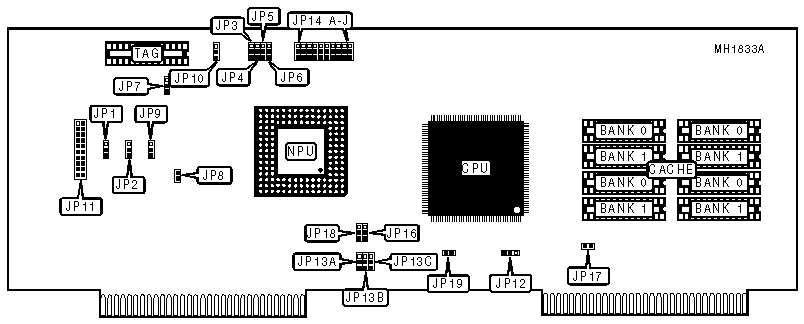
USER CONFIGURABLE SETTINGS |
|||
|
Function |
Jumper |
Position |
|
|
|
2 Clock burst from CPU from cache |
JP1 |
Closed |
|
|
1 Clock burst from CPU from cache |
JP1 |
Open |
|
» |
Factory configured - do not alter |
JP2 |
N/A |
|
» |
Factory configured - do not alter |
JP7 |
N/A |
|
» |
Cache burst mode fill select 4 DWORD line size |
JP8 |
Closed |
|
|
Cache burst mode fill select 1 DWORD line size |
JP8 |
Open |
|
» |
Factory configured - do not alter |
JP10 |
Open |
|
» |
Cache controller IC not installed |
JP11 |
Open |
|
|
Cache controller IC installed |
JP11 |
Closed |
|
|
Non-cached cards using a TTL |
JP12 |
pins 2 & 3 closed |
|
|
Non-cached cards using a Tri-state LBA |
JP12 |
pins 1 & 2 closed |
|
» |
Factory configured - do not alter |
JP16 |
N/A |
|
» |
Factory configured - do not alter |
JP17 |
Open |
|
» |
Factory configured - do not alter |
JP18 |
N/A |
|
» |
Factory configured - do not alter |
JP19 |
N/A |
|
Note: One clock burst operation is not valid for single bank configurations using SRAMs with JP1. |
|||
|
CPU SPEED CONFIGURATION |
|||
|
Speed |
JP9 |
JP15/pins 1 & 2 |
JP15/pins 3 & 4 |
|
16MHz |
Open |
Closed |
Closed |
|
20MHz |
Open |
Open |
Closed |
|
25MHz |
Open |
Closed |
Open |
|
33MHz |
Open |
Open |
Open |
|
40MHz |
Closed |
Open |
Closed |
|
50iMHz |
Open |
Closed |
Open |
|
50MHz |
Closed |
N/A |
N/A |
|
66iMHz |
Open |
Open |
Open |
|
CPU TYPE CONFIGURATION |
|||
|
Type |
JP13A |
JP13B |
JP13C |
|
80486SX |
pins 1 & 2 closed |
pins 1 & 2 closed |
pins 2 & 3 closed |
|
80487SX |
pins 2 & 3 closed |
pins 2 & 3 closed |
Closed |
|
80486DX |
pins 1 & 2 closed |
pins 1 & 2 closed |
pins 2 & 3 closed |
|
80486DX2 |
pins 1 & 2 closed |
pins 1 & 2 closed |
pins 2 & 3 closed |
|
CACHE CONFIGURATION |
|||
|
Size |
Bank 0 |
Bank 1 |
TAG |
|
64KB |
(4) 8K x 8 |
(4) 8K x 8 |
(1) 8K x 8 |
|
128KB |
(4) 32K x 8 |
NONE |
(1) 8K x 8 |
|
256KB |
(4) 32K x 8 |
(4) 32K x 8 |
(1) 32K x 8 |
|
1024KB |
(4) 128K x 8 |
(4) 128K x 8 |
(1) 128K x 8 |
|
CACHE JUMPER CONFIGURATION |
|||||
|
Size |
JP3 |
JP4 |
JP5 |
JP6 |
JP20 |
|
64KB |
pins 1 & 2 |
pins 1 & 2 |
pins 1 & 2 |
pins 1 & 2 |
Open |
|
128KB |
pins 2 & 3 |
pins 1 & 2 |
pins 1 & 2 |
pins 1 & 2 |
Open |
|
256KB |
pins 2 & 3 |
pins 1 & 2 |
pins 2 & 3 |
pins 1 & 2 |
Open |
|
1MB |
pins 2 & 3 |
pins 2 & 3 |
pins 2 & 3 |
pins 2 & 3 |
Open |
|
Note:Pins designated should be in the closed position. |
|||||
|
CACHE JUMPER CONFIGURATION |
||||||||||
|
Size |
JP14A |
JP14B |
JP14C |
JP14D |
JP14E |
JP14F |
JP14G |
JP14H |
JP14I |
JP14J |
|
64KB |
1 & 2 |
2 & 3 |
2 & 3 |
2 & 3 |
2 & 3 |
2 & 3 |
2 & 3 |
2 & 3 |
2 & 3 |
1 & 2 |
|
128KB |
Open |
1 & 2 |
1 & 2 |
1 & 2 |
1 & 2 |
1 & 2 |
1 & 2 |
Open |
Open |
1 & 2 |
|
256KB |
2 & 3 |
2 & 3 |
2 & 3 |
2 & 3 |
2 & 3 |
2 & 3 |
2 & 3 |
Open |
2 & 3 |
1 & 2 |
|
1MB |
2 & 3 |
2 & 3 |
2 & 3 |
2 & 3 |
2 & 3 |
2 & 3 |
2 & 3 |
Open |
2 & 3 |
1 & 2 |
|
Note:Pins designated should be in the closed postion. |
||||||||||