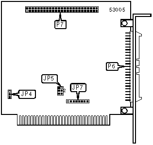
J & J TECHNOLOGY, INC.
JJ.612, JJ.612-1
|
Card Type |
PCMCIA interface |
|
Chip Set |
Unidentified |
|
I/O Options |
PCMCIA Type II slot (JJ.612-1) PCMCIA Type III slot or PCMCIA Type II slots (2) (JJ.612) |
|
Data Bus |
8-bit ISA |

|
CONNECTIONS | |||
|
Function |
Label |
Function |
Label |
|
PCMCIA interface via proprietary connector |
P6 |
PCMCIA interface via 50-pin header |
P7 |
|
Note:A standard PCMCIA slot is provided on an external adapter box. | |||
|
USER CONFIGURABLE SETTINGS | |||
|
Setting |
Label |
Position | |
| » |
Factory configured - do not alter |
JP4 |
Pins 1 & 2 closed |
| » |
Factory configured - do not alter |
JP5 |
Pins 1 & 2, 4 & 5 closed |
| » |
Factory configured - do not alter |
JP7 |
Pins 1 & 2, 5 & 6 closed |
|
Note:JP1 is located under the faceplate of the external PCMCIA drive box. | |||
|
MISCELLANEOUS TECHNICAL NOTES |
|
Note: Three jumpers JP1, JP2 and JP3 are located on the drive unit under the drive unit cover. JP1 sets the base I/O address: 3E0h = open (default) or 1E0h = closed. JP2 and JP3 are factory configured and should not be altered: JP3 = open and JP2/pins 1 & 2 (pins nearest JP3) = closed.
|