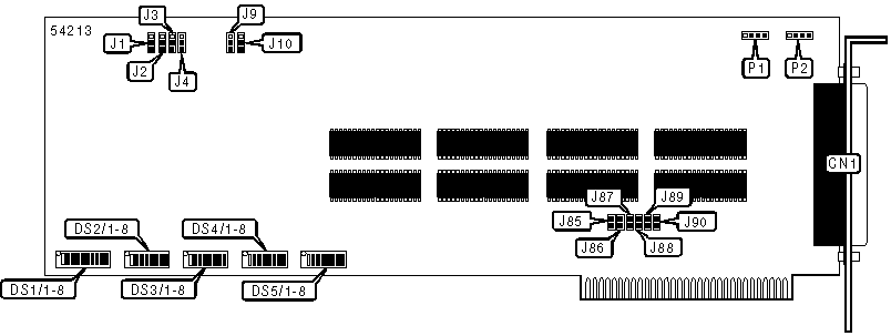
DIGI INTERNATIONAL, INC.
PC/4
|
Card Type |
Serial card |
|
Chip Set |
Unidentified |
|
Maximum Onboard Memory |
Unidentified |
|
I/O Options |
Serial ports (4 RS-232), |
|
Hard Drives supported |
None |
|
Floppy drives supported |
None |
|
Data Bus |
8-bit ISA |
|
Card Size |
Full-length |

|
CONNECTIONS |
|||
|
Function |
Label |
Function |
Label |
|
78-pin cable connector |
CN1 |
Daisy chain cable connector |
P2 |
|
Daisy chain cable connector |
P1 |
|
|
|
Note: Pins 2 & 3 of connectors P1 & P2 are closed when in single board configuration. |
|||
|
USER CONFIGURABLE SETTINGS |
|||
|
Function |
Label |
Position |
|
|
» |
Factory configured - do not alter |
DS1/8 |
On |
|
» |
Factory configured - do not alter |
DS1/9 |
On |
|
|
Interrupt status register enabled |
DS1/10 |
On |
|
|
Interrupt status register disabled |
DS1/10 |
Off |
|
PORT ENABLING SELECTION |
||
|
Port |
Label |
Position |
|
Port 1 enabled |
DS2/8 |
On |
|
Port 1 disabled |
DS2/8 |
Off |
|
Port 2 enabled |
DS3/8 |
On |
|
Port 2 disabled |
DS3/8 |
Off |
|
Port 3 enabled |
DS4/8 |
On |
|
Port 3 disabled |
DS4/8 |
Off |
|
Port 4 enabled |
DS5/8 |
On |
|
Port 4 disabled |
DS5/8 |
Off |
|
BOARD INDENTIFICATION SELECTION |
|||
|
ID |
J9 |
J10 |
|
|
» |
Board 0 |
Pins 2 & 3 closed |
Pins 2 & 3 closed |
|
|
Board 1 |
Pins 2 & 3 closed |
Pins 1 & 2 closed |
|
|
Board 2 |
Pins 1 & 2 closed |
Pins 2 & 3 closed |
|
|
Board 3 |
Pins 1 & 2 closed |
Pins 1 & 2 closed |
|
Note: The primary board in the daisy chain must remain on the default setting. |
|||
|
INTTERRUPT STATUS REGISTER BASE I/O ADDRESS SELECTION |
|||||||
|
Setting |
DS1/1 |
DS1/2 |
DS1/3 |
DS1/4 |
DS1/5 |
DS1/6 |
DS1/7 |
|
000h |
On |
On |
On |
On |
On |
On |
On |
|
008h |
On |
On |
On |
On |
On |
On |
Off |
|
010h |
On |
On |
On |
On |
On |
Off |
On |
|
018h |
On |
On |
On |
On |
On |
Off |
Off |
|
020h |
On |
On |
On |
On |
Off |
On |
On |
|
3D8h |
Off |
Off |
Off |
Off |
On |
Off |
Off |
|
3E0h |
Off |
Off |
Off |
Off |
Off |
On |
On |
|
3E8h |
Off |
Off |
Off |
Off |
Off |
On |
Off |
|
3F0h |
Off |
Off |
Off |
Off |
Off |
Off |
On |
|
3F8h |
Off |
Off |
Off |
Off |
Off |
Off |
Off |
|
Note: A total of 128 base address settings are available. The switches are a binary representation of the decimal memory addresses. DS1/1 is the Most Significant Bit and switch DS1/7 is the Least Significant Bit. The switches have the following decimal values:DS1/1=512, DS1/2=256, DS1/3=128, DS1/4=64, DS1/5=32, DS1/6=16, DS1/7=8. Turn off the switches and add the values of the switches to obtain the correct memory address. (Off=1, On=0) |
|||||||
|
PORT 1 BASE I/O ADDRESS SELECTION |
|||||||
|
Setting |
DS2/1 |
DS2/2 |
DS2/3 |
DS2/4 |
DS2/5 |
DS2/6 |
DS2/7 |
|
000h |
On |
On |
On |
On |
On |
On |
On |
|
008h |
On |
On |
On |
On |
On |
On |
Off |
|
010h |
On |
On |
On |
On |
On |
Off |
On |
|
018h |
On |
On |
On |
On |
On |
Off |
Off |
|
020h |
On |
On |
On |
On |
Off |
On |
On |
|
3D8h |
Off |
Off |
Off |
Off |
On |
Off |
Off |
|
3E0h |
Off |
Off |
Off |
Off |
Off |
On |
On |
|
3E8h |
Off |
Off |
Off |
Off |
Off |
On |
Off |
|
3F0h |
Off |
Off |
Off |
Off |
Off |
Off |
On |
|
3F8h |
Off |
Off |
Off |
Off |
Off |
Off |
Off |
|
Note: A total of 128 base address settings are available. The switches are a binary representation of the decimal memory addresses. DS2/1 is the Most Significant Bit and switch DS2/7 is the Least Significant Bit. The switches have the following decimal values:DS2/1=512, DS2/2=256, DS2/3=128, DS2/4=64, DS2/5=32, DS2/6=16, DS2/7=8. Turn off the switches and add the values of the switches to obtain the correct memory address. (Off=1, On=0) |
|||||||
|
PORT 2 BASE I/O ADDRESS SELECTION |
|||||||
|
Setting |
DS3/1 |
DS3/2 |
DS3/3 |
DS3/4 |
DS3/5 |
DS3/6 |
DS3/7 |
|
000h |
On |
On |
On |
On |
On |
On |
On |
|
008h |
On |
On |
On |
On |
On |
On |
Off |
|
010h |
On |
On |
On |
On |
On |
Off |
On |
|
018h |
On |
On |
On |
On |
On |
Off |
Off |
|
020h |
On |
On |
On |
On |
Off |
On |
On |
|
3D8h |
Off |
Off |
Off |
Off |
On |
Off |
Off |
|
3E0h |
Off |
Off |
Off |
Off |
Off |
On |
On |
|
3E8h |
Off |
Off |
Off |
Off |
Off |
On |
Off |
|
3F0h |
Off |
Off |
Off |
Off |
Off |
Off |
On |
|
3F8h |
Off |
Off |
Off |
Off |
Off |
Off |
Off |
|
Note: A total of 128 base address settings are available. The switches are a binary representation of the decimal memory addresses. DS3/1 is the Most Significant Bit and switch DS3/7 is the Least Significant Bit. The switches have the following decimal values:DS3/1=512, DS3/2=256, DS3/3=128, DS3/4=64, DS3/5=32, DS3/6=16, DS3/7=8. Turn off the switches and add the values of the switches to obtain the correct memory address. (Off=1, On=0) |
|||||||
|
PORT 3 BASE I/O ADDRESS SELECTION |
|||||||
|
Setting |
DS4/1 |
DS4/2 |
DS4/3 |
DS4/4 |
DS4/5 |
DS4/6 |
DS4/7 |
|
000h |
On |
On |
On |
On |
On |
On |
On |
|
008h |
On |
On |
On |
On |
On |
On |
Off |
|
010h |
On |
On |
On |
On |
On |
Off |
On |
|
018h |
On |
On |
On |
On |
On |
Off |
Off |
|
020h |
On |
On |
On |
On |
Off |
On |
On |
|
3D8h |
Off |
Off |
Off |
Off |
On |
Off |
Off |
|
3E0h |
Off |
Off |
Off |
Off |
Off |
On |
On |
|
3E8h |
Off |
Off |
Off |
Off |
Off |
On |
Off |
|
3F0h |
Off |
Off |
Off |
Off |
Off |
Off |
On |
|
3F8h |
Off |
Off |
Off |
Off |
Off |
Off |
Off |
|
Note: A total of 128 base address settings are available. The switches are a binary representation of the decimal memory addresses. DS4/1 is the Most Significant Bit and switch DS4/7 is the Least Significant Bit. The switches have the following decimal values:DS4/1=512, DS4/2=256, DS4/3=128, DS4/4=64, DS4/5=32, DS4/6=16, DS4/7=8. Turn off the switches and add the values of the switches to obtain the correct memory address. (Off=1, On=0) |
|||||||
|
PORT 4 BASE I/O ADDRESS SELECTION |
|||||||
|
Setting |
DS5/1 |
DS5/2 |
DS5/3 |
DS5/4 |
DS5/5 |
DS5/6 |
DS5/7 |
|
000h |
On |
On |
On |
On |
On |
On |
On |
|
008h |
On |
On |
On |
On |
On |
On |
Off |
|
010h |
On |
On |
On |
On |
On |
Off |
On |
|
018h |
On |
On |
On |
On |
On |
Off |
Off |
|
020h |
On |
On |
On |
On |
Off |
On |
On |
|
3D8h |
Off |
Off |
Off |
Off |
On |
Off |
Off |
|
3E0h |
Off |
Off |
Off |
Off |
Off |
On |
On |
|
3E8h |
Off |
Off |
Off |
Off |
Off |
On |
Off |
|
3F0h |
Off |
Off |
Off |
Off |
Off |
Off |
On |
|
3F8h |
Off |
Off |
Off |
Off |
Off |
Off |
Off |
|
Note: A total of 128 base address settings are available. The switches are a binary representation of the decimal memory addresses. DS5/1 is the Most Significant Bit and switch DS5/7 is the Least Significant Bit. The switches have the following decimal values:DS5/1=512, DS5/2=256, DS5/3=128, DS5/4=64, DS5/5=32, DS5/6=16, DS5/7=8. Turn off the switches and add the values of the switches to obtain the correct memory address. (Off=1, On=0) |
|||||||
|
SERIAL PORT INTERRUPT SELECTION |
||||||
|
IRQ |
J85 |
J86 |
J87 |
J88 |
J89 |
J90 |
|
IRQ2 |
Open |
Open |
Open |
Open |
Open |
Closed |
|
IRQ3 |
Closed |
Open |
Open |
Open |
Open |
Open |
|
IRQ4 |
Open |
Open |
Open |
Open |
Closed |
Open |
|
IRQ5 |
Open |
Closed |
Open |
Open |
Open |
Open |
|
IRQ6 |
Open |
Open |
Open |
Closed |
Open |
Open |
|
IRQ7 |
Open |
Open |
Closed |
Open |
Open |
Open |
|
Note: Ports 1-4 must be set to accept either an odd or even interrupt. J1-J4 corresponds to ports 1-4. Place jumper on pins 1 & 2 for an odd interrupt or pins 2 & 3 for an even interrupt. |
||||||