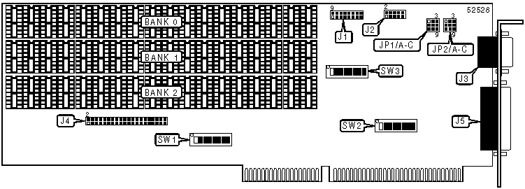
DIAMOND FLOWER, INC.
PBMF-3000
|
Card Type |
Multi-I/O card, |
|
Chip Set |
Unidentified |
|
Maximum Onboard Memory |
3MB DRAM |
|
I/O Options |
Game port, parallel port, serial ports (2), daughter board connector |
|
Data Bus |
16-bit ISA |
|
Floppy drives supported |
None |

|
CONNECTIONS | |||
|
Function |
Label |
Function |
Label |
|
Game port |
J1 |
Daughter board connector |
J4 |
|
Serial port 2 |
J2 |
Parallel port |
J5 |
|
Serial port 1 |
J3 | ||
|
USER CONFIGURABLE SETTINGS | |||
|
Function |
Label |
Position | |
| » |
Serial port 1 DCD normal operation |
JP1 |
Pins 1 & 2 closed |
|
Serial port 1 DCD input forced true |
JP1 |
Pins 2 & 3 closed | |
| » |
Serial port 1 DSR normal operation |
JP1 |
Pins 4 & 5 closed |
|
Serial port 1 DSR input forced true |
JP1 |
Pins 5 & 6 closed | |
| » |
Serial port 1 CTS normal operation |
JP1 |
Pins 7 & 8 closed |
|
Serial port 1 CTS input forced true |
JP1 |
Pins 8 & 9 closed | |
| » |
Serial port 2 DCD normal operation |
JP2 |
Pins 1 & 2 closed |
|
Serial port 2 DCD input forced true |
JP2 |
Pins 2 & 3 closed | |
| » |
Serial port 2 DSR normal operation |
JP2 |
Pins 4 & 5 closed |
|
Serial port 2 DSR input forced true |
JP2 |
Pins 5 & 6 closed | |
| » |
Serial port 2 CTS normal operation |
JP2 |
Pins 7 & 8 closed |
|
Serial port 2 CTS input forced true |
JP2 |
Pins 8 & 9 closed | |
| » |
Parity enabled |
SW1/8 |
On |
|
Parity disabled |
SW1/8 |
Off | |
| » |
Game port enabled |
SW2/4 |
On |
|
Game port disabled |
SW2/4 |
Off | |
| » |
Factory configured - do not alter |
SW3/7 |
Unidentified |
| » |
Factory configured - do not alter |
SW3/8 |
Unidentified |
|
DRAM SWITCH CONFIGURATION | |||||||||
|
Size |
Bank 0 |
Bank 1 |
Bank 2 |
Bank 3 |
Bank 4 |
Bank 5 |
SW2/1 |
SW2/2 |
SW2/3 |
|
256KB |
4164 |
None |
None |
None |
None |
None |
Off |
Off |
off |
|
512KB |
4164 |
4164 |
None |
None |
None |
None |
On |
Off |
Off |
|
384KB |
4164 |
4164 |
4164 |
None |
None |
None |
Off |
On |
Off |
|
512KB |
4164 |
4164 |
4164 |
4164 |
4164 |
4164 |
On |
On |
Off |
|
512KB |
41256 |
None |
None |
None |
None |
None |
Off |
Off |
On |
|
1024KB |
41256 |
41256 |
None |
None |
None |
None |
On |
Off |
On |
|
1536KB |
41256 |
41256 |
41256 |
None |
None |
None |
Off |
On |
On |
|
2048KB |
41256 |
41256 |
41256 |
41256 |
41256 |
41256 |
On |
On |
On |
|
Note: Banks 3, 4 and 5 are located on the expansion board. Each bank takes 18 chips of the designated size. | |||||||||
|
MEMORY SWITCH CONFIGURATION | ||||||||
|
Address |
Size |
SW1/1 |
SW1/2 |
SW1/3 |
SW1/4 |
SW1/5 |
SW1/6 |
SW1/7 |
|
20000h |
256KB |
On |
Off |
Off |
Off |
Off |
Off |
Off |
|
40000h |
512KB |
Off |
On |
Off |
Off |
Off |
Off |
Off |
|
60000h |
1MB |
On |
On |
Off |
Off |
Off |
Off |
Off |
|
80000h |
1.125MB |
Off |
Off |
On |
Off |
Off |
Off |
Off |
|
100000h |
1.25MB |
On |
Off |
On |
Off |
Off |
Off |
Off |
|
F60000h |
15.375MB |
On |
On |
Off |
On |
On |
On |
On |
|
F80000h |
15.5MB |
Off |
Off |
On |
On |
On |
On |
On |
|
FA0000h |
15.675MB |
On |
Off |
On |
On |
On |
On |
On |
|
FC0000h |
15.75MB |
Off |
On |
On |
On |
On |
On |
On |
|
FE0000h |
15.875MB |
On |
On |
On |
On |
On |
On |
On |
|
Note: A total of 127 base address settings are available. The switches are a binary representation of the decimal memory addresses. SW1/7 is the Most Significant Bit and switch SW1/1 is the Least Significant Bit. The switches have the following decimal values: SW1/7=8388608, SW1/6=4194304, SW1/5=2097152, SW1/4=1048576, SW1/3=524288, SW1/2=262144, SW1/1=131072. Turn off the switches, add the values of the switches, and convert to hexadecimal to obtain the correct memory address. (Off=1,On-0). To obtain the Kilobyte memory size, divide the decimal value of the memory address by 1024, and to obtain the megabyte size divide by 1024 again. | ||||||||
|
PORT CONFIGURATION | ||
|
Setting |
SW2/7 |
SW2/8 |
|
Disabled |
Off |
Off |
|
Disabled |
On |
On |
|
LPTA |
Off |
On |
|
LPTB |
On |
Off |
|
SERIAL PORT 1 & 2 ADDRESS SELECTION | ||||
|
Serial port 1 |
Serial port 2 |
SW2/5 |
SW2/6 | |
|
Disabled |
Disabled |
Off |
Off | |
| » |
COM1 (3F8h) |
COM2 (2F8h) |
Off |
On |
|
COM2 (2F8h) |
COM3 (3E8h) |
On |
Off | |
|
COM3 (3E8h) |
COM4 (2E8h) |
On |
On | |
|
SERIAL PORT 1 INTERRUPT SELECTION | |||
|
IRQ |
SW3/3 |
SW3/4 | |
|
IRQ3 |
On |
Off | |
| » |
IRQ4 |
Off |
On |
|
Disabled |
Off |
Off | |
|
SERIAL PORT 2 INTERRUPT SELECTION | |||
|
IRQ |
SW3/1 |
SW3/2 | |
| » |
IRQ3 |
On |
Off |
|
IRQ4 |
Off |
On | |
|
Disabled |
Off |
Off | |
|
PARALLEL PORT INTERRUPT SELECTION | |||
|
IRQ |
SW3/5 |
SW3/6 | |
|
Disabled |
Off |
Off | |
| » |
IRQ7 |
Off |
On |
|
IRQ5 |
On |
Off | |
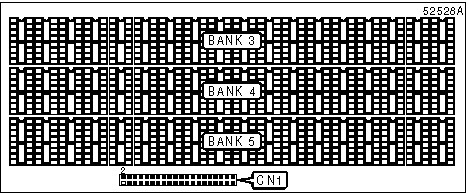
DIAMOND FLOWER, INC.
PBMF-3000 DAUGHTER BOARD

|
CONNECTIONS | |
|
Function |
Label |
|
Daughter board connector |
CN1 |